
Researchers have developed a method to significantly improve the surface quality of micro-optical components made using femtosecond laser-induced chemical etching (FLICE). The study, published in Scientific Reports, focuses on fused silica micro-lenses—small optical elements used in devices such as cameras, sensors, and medical imaging systems.
What Happened
The team applied inert gas atmospheric pressure plasma (AP plasma) post-processing to micro-lenses created through FLICE. FLICE uses ultra-short laser pulses to etch precise patterns into fused silica, a material known for its optical clarity and stability. However, the resulting surfaces often exhibit high surface roughness, which degrades light transmission and increases scattering.
Using a plasma discharge of inert gases—such as argon or nitrogen—at atmospheric pressure, the researchers polished the surfaces of these micro-lenses. The process was conducted at a controlled gap distance and with specific power input. After treatment, the average surface roughness (Ra) dropped from 0.207 ± 0.044 micrometers to 0.047 ± 0.018 micrometers—a reduction of over 75%—while preserving the original lens geometry.
Key Facts
- The surface roughness reduction was verified using optical profilometry and interferometry, standard techniques for measuring surface topography.
- Light scattering measurements confirmed that polished surfaces transmitted light more efficiently than unpolished ones.
- Optimal performance occurred at a discharge gap of 5 mm and a plasma power of 5.5 W.
- Higher power or larger gap distances led to plasma instability and inhomogeneity, reducing polishing efficiency.
- The method does not alter the lens shape or optical function, making it suitable for precision applications.
How It Works: Background and Process
Femtosecond laser-induced chemical etching (FLICE) works by directing ultra-short laser pulses at a fused silica surface. These pulses trigger localized chemical reactions that remove material in a controlled, non-thermal manner. The result is high-precision etching with fine features, but the surface often remains rough due to the chemical reaction dynamics and residual byproducts.
Atmospheric pressure plasma is generated by applying a high voltage across two electrodes separated by a gap, with an inert gas (like argon) flowing between them. When the voltage exceeds a threshold, the gas ionizes, forming a plasma that emits energetic particles and UV radiation. These components interact with the surface of the micro-lens, removing microscopic irregularities through a physical sputtering and chemical interaction mechanism.
Unlike traditional polishing methods that require mechanical contact or liquid abrasives, this plasma method operates in air at ambient pressure. This eliminates the need for vacuum chambers or complex fluid handling, reducing cost and enabling scalable processing. The plasma’s energy is focused on surface features, enabling selective smoothing without damaging the underlying structure.
Why It Matters
High surface roughness in optical components leads to increased light scattering, which degrades image quality and reduces system sensitivity. In applications such as endoscopic imaging, augmented reality, or high-resolution sensors, even minor scattering can significantly impact performance.
This plasma post-processing technique offers a scalable, non-contact, and low-cost solution to improve surface finish without altering the lens’s design. Because it preserves the original geometry, it is compatible with existing fabrication workflows. The method also avoids the use of consumables like polishing compounds or mechanical tools, reducing waste and contamination risks.

For industries relying on precision optics—such as medical diagnostics, aerospace sensors, or consumer electronics—this advancement could lead to more reliable and cost-effective optical components.
Limitations and Open Questions
While the results are promising, the study is limited in scope. The research was conducted under controlled laboratory conditions using a specific setup and material. The effectiveness of the method has not yet been tested on a broader range of materials or in real-world manufacturing environments.
Key open questions remain: How does the process perform on lenses with complex shapes or varying curvature? What is the long-term stability of the polished surface under environmental exposure or thermal cycling? How does the method scale to larger or higher-volume production?
Additionally, the study does not address potential material degradation or the formation of secondary byproducts during plasma exposure. These factors could influence the durability and repeatability of the process in industrial settings.
What to Watch Next
Future work should focus on validating the method across different lens geometries and materials. Researchers may explore variations in gas type, pressure, or electrode design to optimize performance for specific applications.
Integration with automated fabrication lines could enable real-time monitoring and control of surface quality. Additionally, combining this plasma polishing with other optical fabrication techniques—such as lithography or 3D printing—could open new pathways for hybrid optical component design.
For readers interested in the intersection of advanced materials and precision optics, quantum optical components and material performance under environmental stress offer complementary perspectives on how surface engineering impacts functionality and reliability.
The original research is available at Scientific Reports.
Sources & further reading
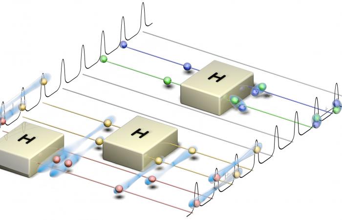
Featured image: The team’s quantum frequency processor operates on photons (spheres) through quantum gates (boxes), synonymous with classical circuits for quantum computing. Superpositions are shown by spheres straddling multiple lines; entanglements are visualized as clouds. Credit: Andy Sproles/ORNL, U.S. Dept. of Energy
www.ornl.gov/news/researchers-demonstrate-new-building-bl… by Oak Ridge National Laboratory, CC BY 2.0, via Wikimedia Commons. Image source · License